


제목
An Innovation in Transparent Flexible Electronic Materials
Office of Information | 2018-11-23 | 조회 11983
본문 내용
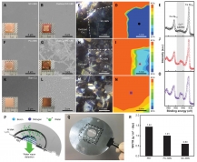
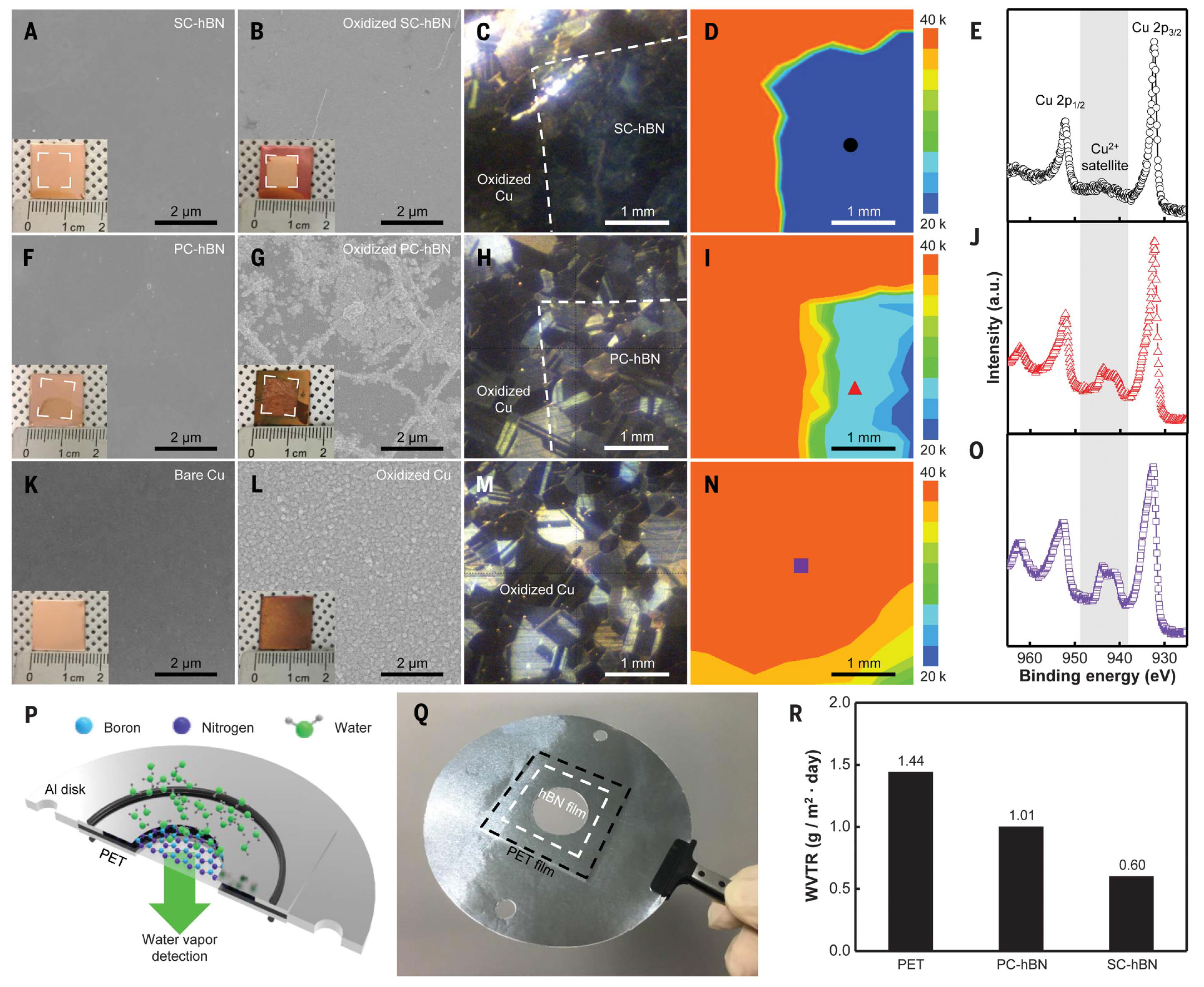
Among two-dimensional materials, hexagonal boron nitride (hBN) is the only insulating material that is used to make transparent flexible and wearable electronic products. However, the large-area ‘polycrystalline hexagonal boron nitride’ synthesized by the conventional method has shown a low insulating character due to its incomplete atomic bonding of boron and nitrogen.
For the first time in history, Joo Song Lee (BIN Fusion Engineering doctoral student at Chonbuk National University) and his team have successfully discovered a way to synthesize wafer-scale ‘single-crystalline hexagonal boron nitride’ (SC-hBN) monolayer films with chemical vapor deposition, and have published the results of the study in Science magazine recently as the main author.
What is remarkable is the researchers opened the possibility of transforming heterogeneous multilayered 2D materials into large-area monolayered ones.
Lee’s team synthesized a thin monocrystalline boron nitride film on a large liquid gold surface by using self-collimation of hBN grains where the grains are formed in the same crystal direction. In this way, the single crystals can be synthesized into unlimited sizes.
Single-crystal two-dimensional materials are considered to be key materials for next-generation transparent electronic products, as they have excellent electrical characteristics, flexibility and transparency. In addition, they don’t transmit gas, thus are highly utilizable as a gas barrier of organic electronic devices.
This technology is expected to revolutionize the development of future electronic devices, gas barriers, sensors and filters that are transparent and at the same time flexible.


